The following figure shows the bit definitions for read and write operations to this port.
Read
+-----------------------------------------------+
| 7 | 6 | 5 | 4
| 3 | 2 | 1 | 0 |
|-----+-----+-----+-----+-----+-----+-----+-----|
| P | CHK | OT2 | REF | DCK | DP | SPK | GT2
|
+-----------------------------------------------+
Write
+-----------------------------------------------+
| 7 | 6 | 5 | 4
| 3 | 2 | 1 | 0 |
|-----+-----------------+-----+-----+-----+-----|
| RT0 | Reserved | DCK
| DP | SPK | GT2 |
+-----------------------------------------------+
P: Parity check
RT0: Reset timer 0
CHK: Channel check
OT2: Timer 2 output
REF: Refresh request toggle
DCK: Disable channel check
DP: Disable parity check
SPK: Enable speaker data
GT2: Timer 2 gate to speaker
P The parity-check bit (bit 7) is a read-only bit that indicates whether a parity error was detected. When the bit is 1, a parity error was detected.
RT0 The reset-timer-0 bit is a write-only bit that is used to reset the timer-tick interrupt (timer 0 output). Setting this bit to 1 resets the output of timer 0 and IRQ0. Setting this bit to 0 has no effect. (See the definition of the parity-check bit.)
CHK The channel-check bit (bit 6) is a read-only bit that indicates if a channel-check condition has occurred. When this bit is a 1, a channel-check condition has occurred.
OT2 The timer-2-output bit (bit 5) is a read-only bit that reflects the state of the output from timer 2 (tone generator).
REF The refresh-request bit (bit 4) is a read-only bit that toggles for memory refresh request.
DCK The disable-channel-check bit is used to enable and disable nonmaskable interrupts when a channel-check condition is detected. When this bit is set to 0, channel checks are enabled. It is set to 1 during POST and reset to 0 after POST has been completed.
DP The disable-parity-check bit (bit 2) is used to enable and disable nonmaskable interrupts caused by parity errors. When this bit is set to 0, parity checks are enabled. It is set to 1 during POST and reset to 0 after POST has been completed.
SPK The enable-speaker-data bit (bit 1) is used to enable and disable the output to the speaker. When this bit is set to 1, speaker data is enabled.
GT2 The timer-2-gate bit (bit 0) is used to enable and disable timer 2. When this bit is set to 1, the timer 2 is enabled.
RTC Address and NMI Mask Register (Hex0070)
This register is used with the RTC Data register (hex 0071) to read from and write to the RT/CMOS RAM bytes.
Warning: The operation following a write operation to this register must access the RT/CMOS Data register (hex 0071); otherwise, intermittent malfunctions and unreliable operation of the RT/CMOS RAM can occur.
+-----------------------------------------------+
| 7 | 6 | 5 | 4
| 3 | 2 | 1 | 0 |
|-----+-----------------------------------------|
| NMI |
Address
|
+-----------------------------------------------+
NMI: NMI mask
ADDRESS: RT/CMOS RAM address
NMI The NMI-mask bit is a read/write bit that is used to enable and disable nonmaskable interrupts. Setting this bit to 1 disables (or masks) the NMI (see Nonmaskable Interrupt). Setting this bit to 0 enables the NMI. This bit is set to 1 during a power-on reset, but it is reset to 0 before POST is completed.
Address The address field is a write-only field that specifies the address within the RT/CMOS data area that is accessed through the RT/CMOS Data register.
RTC
Data Register (Hex0071)
This register is used with the RTC Address and NMI Mask register to
read from and write to the nonvolatile RAM data area.
+-----------------------------------------------+
| 7 | 6 | 5 | 4
| 3 | 2 | 1 | 0 |
|-----------------------------------------------|
|
RT/CMOS data
|
+-----------------------------------------------+
System Control Port C (Hex007C)
This read/write register is used to enable the secure media mode (see
Secure Media Mode).
Note: When writing to this register,
1. Read the register to ensure that bit 7 is 0.
2. Change only the enhanced-command bit.
3. Write the new value to the register.
+-----------------------------------------------+
| 7 | 6 | 5 | 4
| 3 | 2 | 1 | 0 |
|-----+-----------------------------------+-----|
| TIP |
Reserved
| ENC |
+-----------------------------------------------+
TIP: Transfer in progress
ENC: Enhanced command/status
TIP The transfer-in-progress bit (bit 7) is a read-only bit that indicates whether the EEPROM is in the process of transferring data. While a transfer is in progress, this register is busy and must not be modified.
When this bit is 1, the EEPROM is in the process of transferring data, and the register is not available to be modified. When this bit is 0, a transfer is not in progress, and the contents of register can be safely modified.
ENC
The enhanced-command/status bit (bit 0) controls the state of the -security
cmd signal to the diskette drive connector. This signal is used to
place the diskette drive in the secure media mode in order to issue enhanced
commands to the drive and to retrieve enhanced status. The mode and
commands require that both the drive and diskette drive controller support
this signal.
When the bit is set to 0, the -security cmd
signal is driven active (low).
When the bit is set to 1, the signal is driven
inactive (high).
Changing the -security cmd signal from active to inactive (bit 0 is reset to 1) issues an enhanced command to the selected drive.
Central Arbiter Register (Hex0090)
The central-arbitration control-point provides access to programmable options through the Arbitration register, which is at I/O address hex 0090.
Read
+-----------------------------------------------+
| 7 | 6 | 5 | 4
| 3 | 2 | 1 | 0 |
|-----+-----+-----+-----+-----------------------|
| EPC | NMI | BTO | R |
Arb Level |
+-----------------------------------------------+
Write
+-----------------------------------------------+
| 7 | 6 | 5 | 4
| 3 | 2 | 1 | 0 |
|-----+-----+-----------------------------------|
| EPC | MSK |
Reserved
|
+-----------------------------------------------+
EPC: Enable processor cycle
MSK: Arbitration mask
R: Reserved
NMI: NMI occurred
BTO: Bus time-out
EPC The enable-processor-cycle bit controls whether the system microprocessor can use the channel while other devices are arbitrating for control. When this bit is set to 1, the system microprocessor can transfer data on the system bus while ARB/-GNT is in the ARB state. This bit can be set to 0 if an arbitrating device requires total control of the channel bandwidth. The power-on self-test (POST) sets this bit to 1.
MSK The arbitration-mask bit is a write-only bit that enables and disables the central-arbitration-control-point. Setting this bit to 1 causes the central-arbitration-control-point to enter the arbitration state, which forces ARB/-GNT to the ARB state. The system microprocessor controls the channel until this bit is reset to 0 by a system reset.
Warning: This bit should be set to 1 only by diagnostic routines and system error-recovery routines.
NMI The NMI-occurred bit is a read-only bit that indicates whether an NMI was detected. When an NMI occurs, the central-arbitration-control-point is forced into the arbitration state, which prevents any bus-masters from getting control of the channel. Reading this register reset this bit to 0.
BTO The bus-time-out bit is a read-only bit that indicates whether the NMI was caused by a bus timeout or some other reason. If the bit is 1, the NMI was caused by a bus time-out. If the bit is 0, the NMI is caused by another error. Reading this register resets this bit to 0.
EXT The enable-extended-arbitration bit is a write-only bit that controls the minimum arbitration cycle. When this bit is set to 0, the minimum arbitration cycle is 300 nanoseconds; setting this bit to 1 extends that minimum cycle to 600 nanoseconds. POST sets this bit to 0.
ARB The arbitration-level bits are read-only bits that indicate the arbitration level of the arbiter that was granted control of the channel during the most recent arbitration cycle. This information allows the system microprocessor to determine the arbitration level of the device that caused a bus time-out.
Card
Selected Feedback register (Hex0091)
The Card Selected Feedback register is a read-only register at address
hex 0091. It allows programs to monitor the '-card selected feedback' signal
(-CD SFBK). When an adapter is addressed, it responds by driving this signal
active. Diagnostic and
configuration programs use this signal to verify the operation of an
adapter at a given address or DMA port.
+-----------------------------------------------+
| 7 | 6 | 5 | 4
| 3 | 2 | 1 | 0 |
|-----------------------------------------+-----|
|
Reserved
| SFB |
+-----------------------------------------------+
SFB: Card selected feedback
SFB When the card-selected-feedback bit (bit 0) is 1, the -CD SFBK signal from an adapter in the channel was active on a previous cycle or a system board I/O function (diskette drive, serial port, or parallel port) was accessed by an I/O cycle. Reading this register resets the bit to 0.
System
Control Port A (Hex0092)
+---------------------------------------------------------------+
| 7 | 6 |
5 | 4 | 3 |
2 | 1 | 0 |
|-----------------------+-------+-------+-------+-------+-------|
| Reserved
| WD | SEC | R |
A20 | ARS |
+---------------------------------------------------------------+
WD: Watchdog-timer status
SEC: Security lock
R: Reserved
A20: Alternate gate A20
ARS: Alternate hot reset
WD The watchdog-timer-status bit (bit 4) is a read-only bit that indicates the status of the watchdog timer. When this bit is 1, a watchdog time-out has occurred. For more information about the watchdog timer, refer to Programmable Timers in the IBM Personal System/2 Hardware Interface Technical Reference--Common Interfaces.
SEC The security-lock bit (bit 3) provides the security lock for the secured area of RT/CMOS RAM that hold the power-on password. When this bit is set to 1, the 8-byte password is electronically locked. POST sets this bit; it can be cleared only by turning the system off.
A20 The gate-A20 bit (bit 1) is ORed with bit 1 in the Keyboard Output port to enable the 'address 20' line (A20). When both bits are set to 0, A20 is disabled and is always 0. This bit is set to 0 during POST.
ARS The alternate-hot-reset bit (bit 0) provides an alternative method of resetting the system microprocessor. Resetting the system microprocessor switches the microprocessor from protected mode to real-address mode. The alternative reset takes 13.4 microseconds.
This bit is set to 0 by either a system reset or a write operation. When a write operation changes this bit from 0 to 1, the alternative reset pin is pulsed high for 100 to 125 nanoseconds. The reset occurs after a minimum delay of 6.72 microseconds. While the reset is occurring, the latch remains set so that POST can read the state of this bit. If this bit is 1, POST assumes that the microprocessor is being switched from protected mode to real mode.
When using this bit to reset the system microprocessor to real mode, use the following procedure:
1. Disable all maskable and nonmaskable interrupts.
2. Reset the system microprocessor by setting the
bit to 1.
3. Issue a Halt instruction to the system microprocessor.
4. Reenable all maskable and nonmaskable interrupts.
Note: Whenever possible, use advanced BIOS (ABIOS) to reset the system to real mode.
System
Board Enable/Setup Register (Hex 0094)
This read-write register is used to place the system board functions
into setup mode
and to select which group of registers is accessed during setup.
Configure only one
group at a time.
Note: Ensure that all bits are set
to 1 when not performing setup on a system board function.
+----------------------------------------------+
| 7 | 6 | 5 | 4 |
3 | 2 | 1 | 0 |
|----+-----+-----------------------+-----+-----|
|GRP1| GRP2| Reserved
| GRP3| R |
+----------------------------------------------+
GRP1: Enable/setup group 1
GRP2: Enable/setup group 2
GRP3: Enable/setup group 3
GRP1 When this bit is set to 0, the diskette drive controller and parallel port B are placed in setup mode, and the group 1 functions are accessed.
GRP2 When this bit is set to 0, the system board serial ports are placed in setup mode, and the group 2 functions are accessed.
GRP3 When this bit is set to 0, the high-speed parallel port is placed in setup mode, and group 3 functions are accessed.
Adapter
Enable/Setup Register (Hex 0096)
This read/write register resets the channel, enables the respective
'-card setup' signal to configure adapters in the channel.
+-----------------------------------------------+
| 7 | 6 | 5 | 4
| 3 | 2 | 1 | 0 |
|-----+-----+-----+-----+-----+-----------------|
| RST | 0 | 0 | 0 | STUP|
Select |
+-----------------------------------------------+
RST: Channel reset
SELECT: Channel select
STUP: Enable card setup
RST When this bit is set to 1, the 'channel reset' signal is activated to all connectors.
STUP The card-setup bit determines whether the '-card setup' signal is driven active. This signal is used to put an adapter into the setup mode. When this bit is set to 1, the signal is driven active for the connector specified by the channel-select bits. When this bit is set to 0, the signal is gated off.
Select The channel-select bits determine which channel
connector is put into the setup mode when the '-card setup' signal is driven
active. Connectors 1 through 8 are addressed as 0 through 7.
Note:
-CD SETUP goes active only when the microprocessor performs an I/O operation
in the address range 0100h through 0107h.
Operator
Panel Registers (Hex0108-010F)
The operator panel has an eight-character display that can be used
to indicate operator messages and display system status when the video
display is turned off (in server environments, using the display on the
operator panel allows the video display to be turned off, thereby reducing
the power consumed).
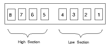
The eight positions on the operator-panel display are numbered right to left.
Operator Panel Position Numbering
Eight write-only registers provide a means of writing characters to
each position.
Operator Panel Register 1 (address 0108h) defines the character in
position 1.
Operator Panel Register 8 (address 010Fh) defines the character at
position 8.
The Character field can select one of 128 characters from 00 to 7Fh;
bit 7 is
reserved. The character codes 20h through 7Eh are the standard
ASCII characters.
Operator Panel Register
+-----------------------------------------------+
| 7 | 6 | 5 | 4
| 3 | 2 | 1 | 0 |
|-----+-----------------------------------------|
| R |
Character
|
+-----------------------------------------------+
For example, to write the number 307 in the display panel starting at the left-most position:
o Write 33h to Operator Panel Register 8 (010Fh)
o Write 30h to Operator Panel Register 7 (010Eh)
o Write 37h to Operator Panel Register 6 (010Dh)