| Introduction | Buses | Modules | Systems | Chips | Miscellany |
It is the CMTU that interfaces to the MBus, thus in many places (bug-reports, PROM banner, Solaris messages file, Sun patch-reports, etc.), such modules are described as "RT625" or "RT626" modules.
Worse, the term RT625 is sometimes also used to stand for RT626! For instance, the SPARCstation-20 PROM banner displayed at powerup may claim to have "4 x RT625" even when fitted with modules equipped with RT626 chips.
Thus there is often confusion as to what "RT625" and "RT626" mean - sometimes the term is used to refer to a specific CMTU chip, sometimes to refer to any HyperSPARC CMTU chip, and sometimes is used to refer (somewhat incompletely) to the MBus module as a whole.
I always use the former interpretation.
| Code Name | Chip Name | L1 I-cache | L1 D-cache | Silicon Die feature size | Known Speeds (MHz) |
|---|---|---|---|---|---|
| Colorado-1 | RT620A | 8 Kb | none | 0.5 micron | 55, 60, 72, 80 |
| Colorado-2 | RT620B | 8 Kb | none | 0.4 micron | 90, 100, 110, 125 |
| Colorado-3 | RT620C | 8 Kb | none | 0.35 micron | 110, 125, 133, 142, 150, 166 |
| Colorado-4 | RT620D | 16 Kb | 16 Kb | 0.35 micron TLM (triple-layer-metal) |
180, x4, x4.5 |
"Known Speeds" does not exclude other possibilities. As far as is known, all dual-CPU HyperSPARC modules use a pair of identical-series CPUs (ie: both RT620B or both RT620C).
The A, B, and C revs of the RT620 differ mainly in the manufacturing process of the IC dies - as Fujitsu progressed down a path of smaller-feature-size silicon-wafer production-lines.
However, the RT620D must have been somewhat of a redesign - there were substantial architectural differences (much larger L1 instruction-cache, and now with a data-cache too!).
Note also that the RT620D requires a different CMTU to the earlier CPUs (presumably to cater for the L1 D-cache on the CPU and the half-speed L2 cache). Whether that CMTU is a slight revision of the RT626A (ie: RT626B?), or is a new IC design with some other designation is not clear (unless you know better).
| Chip Name | Max L2 Cache | Max MBus Clock |
|---|---|---|
| RT625 | 256? Kb | 55 MHz |
| RT626 | 1024 Kb | 75 MHz in principle (but see Ross HS30) |
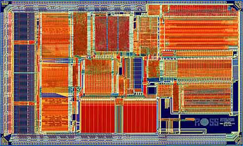
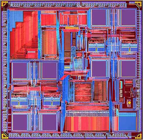
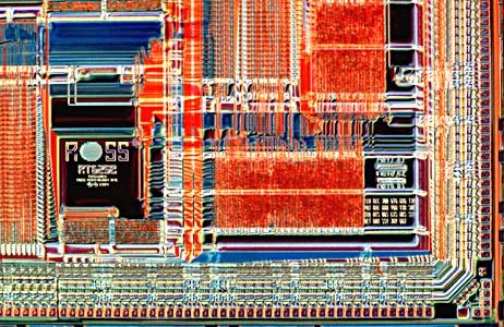
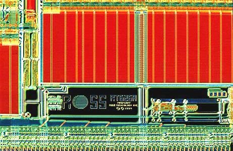
Judging from chip micrographs, the the RT625C and RT626A appear to have completely different IC layouts. This makes sense, because the RT626 was designed to support programmable MBus frequencies upto 75MHz and other advanced features of the Ross RT521/523 system-level chipset.
All HyperSPARC modules with 512Kb or more of external cache use an RT626 CMTU; the others probably all use an RT625 CMTU.
The RT627 is a 64Kb RAM (four chips needed for a 256Kbyte cache), whereas the RT628 is 128Kb (two chips needed for a 256Kbyte cache).
I have no revsion information for these chips. It hardly matters :-).
| Introduction | Buses | Modules | Systems | Chips | Miscellany |
| Mike Spooner, revised 9th May 2006 |